RF Design and RF Components Design Services Circuit Diagram Prototyping and Testing. Crafting a prototype stands as a pivotal milestone in the intricate dance of radio frequency design. Picture this: engineers diligently gathering an array of essential components—circuit boards, RF modules, power supplies—their minds racing with possibilities. Discover the essentials of RF circuit design with RF Engineer's comprehensive beginner's guide. Explore key concepts, including frequency selection, impedance matching, and circuit components. Master the fundamentals of RF circuit design to build effective communication systems. Learn the critical aspects of designing RF circuits, focusing on their practical applications and inherent challenges. This module will introduce the student to the RF and mm-Wave Circuit Design course and to the topic of wireless systems. It will present the learning objectives, grading system, supporting material, introductory class, and design labs. Besides, it will show the student how to use the simulation tools and the equipment used in the design labs.

RF Circuit Design Basic Steps. Start by developing a comprehensive specification for the design, detailing functions and key parameters. This includes the required gain and noise figure of the Low Noise Amplifier (LNA), the output power of the Power Amplifier (PA), the phase noise of the Local Oscillator (LO), and the conversion gain of the mixer. RF circuit design is a specialized field that combines electromagnetic theory with electrical engineering principles. By optimizing signal propagation, impedance matching, and PCB layouts, engineers can develop efficient and high-performance RF systems for a wide range of applications, from cutting-edge communication networks to advanced radar

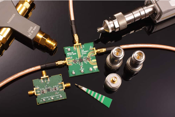
What is RF Circuit Design? Circuit Diagram
The RF circuit of the transmitter can convert and up-convert the processed baseband signal to the specified channel and inject this signal into the transmission medium. Conversely, the RF circuit of the receiver can obtain the signal from the transmission medium and convert and down-convert it to the baseband.

Figure 1: General Equivalent Circuits for RF Oscillators The procedure is to design an active negative resistance circuit which, under large-signal steady-state conditions, exactly cancels out the load and any other positive resistance in the closed loop circuit. This leaves the equivalent circuit represented by a single L and C in either
What is RF Circuit Design? Circuit Diagram
RF circuit variability, both manufacturing and design induced, must be modeled, and compensated for. In analog design, circuit stimulus is treated as a continuously varying signal over time. In the context of wireless communications, analog design often refers to the "low frequency" or "baseband" circuit as opposed to the "RF" circuit.